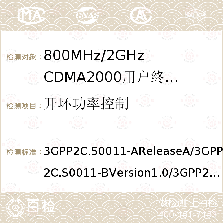
1、在上一篇的probe函数中,在那个很大的for循环中出现了,对NAND的厂商,设备号,是MLC或SLC进行判断,这些是怎样进行的呢?
其实这些都是在NAND芯片中定义的,我们只需按对应的时序读出这些信息,就可以进行判断,看下面这个图(摘于一个NAND芯片手册):
2、上一篇中,nand_scan(s3c_mtd, 1)函数没有细说,这一篇说下这个函数,源码如下:
/**
* nand_scan - [NAND Interface] Scan for the NAND device
* @mtd: MTD device structure
* @maxchips: Number of chips to scan for
*
* This fills out all the uninitialized function pointers
* with the defaults.
* The flash ID is read and the mtd/chip structures are
* filled with the appropriate values.
* The mtd->owner field must be set to the module of the caller
*
*/
int nand_scan(struct mtd_info *mtd, int maxchips)
{
int ret;
/* Many callers got this wrong, so check for it for a while... */
if (!mtd->owner && caller_is_module()) {
printk(KERN_CRIT "nand_scan() called with NULL mtd->owner!n");
BUG();
}
ret = nand_scan_ident(mtd, maxchips);
if (!ret) 如果上面的函数成功,这执行nand_scan_tail函数。这个函数的分析,看下面:
ret = nand_scan_tail(mtd);
return ret;
}
主要就是上面那个函数:nand_scan_ident,源码如下:
/**
* nand_scan_ident - [NAND Interface] Scan for the NAND device
* @mtd: MTD device structure
* @maxchips: Number of chips to scan for
*
* This is the first phase of the normal nand_scan() function. It
* reads the flash ID and sets up MTD fields accordingly.
*
* The mtd->owner field must be set to the module of the caller.
*/
int nand_scan_ident(struct mtd_info *mtd, int maxchips)
{
int i, busw, nand_maf_id;
struct nand_chip *chip = mtd->priv; 得到struct nand_chip结构体
struct nand_flash_dev *type;
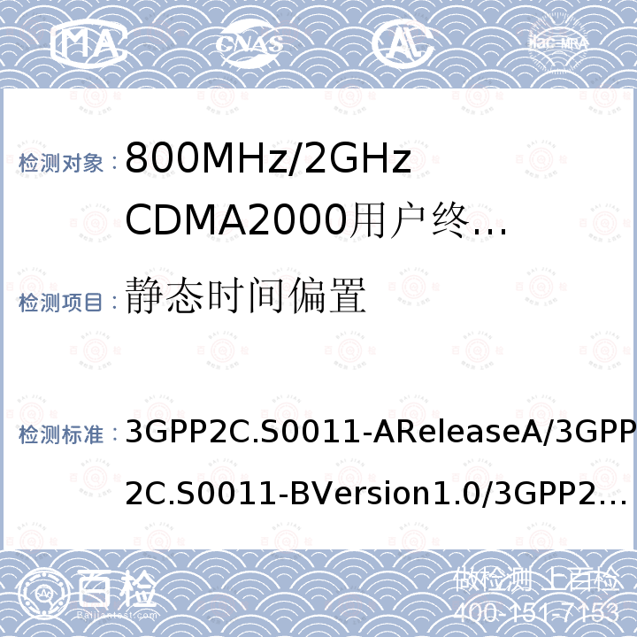
/* Get buswidth to select the correct functions */
busw = chip->options & NAND_BUSWIDTH_16; 和数据宽度有关,看下面这个图:
/* Set the default functions */ 根据数据宽度设置默认函数:
nand_set_defaults(chip, busw);此函数源码如下:
/*
* Set default functions
*/
static void nand_set_defaults(struct nand_chip *chip, int busw)
{
/* check for proper chip_delay setup, set 20us if not */
if (!chip->chip_delay)
chip->chip_delay = 20;
/* check, if a user supplied command function given */
if (chip->cmdfunc == NULL)
chip->cmdfunc = nand_command;
/* check, if a user supplied wait function given */
if (chip->waitfunc == NULL)
chip->waitfunc = nand_wait;
if (!chip->select_chip)
chip->select_chip = nand_select_chip;
if (!chip->read_byte)
chip->read_byte = busw ? nand_read_byte16 : nand_read_byte;
if (!chip->read_word)
chip->read_word = nand_read_word;
if (!chip->block_bad)
chip->block_bad = nand_block_bad;
if (!chip->block_markbad)
chip->block_markbad = nand_default_block_markbad;
if (!chip->write_buf)
chip->write_buf = busw ? nand_write_buf16 : nand_write_buf;
if (!chip->read_buf)
chip->read_buf = busw ? nand_read_buf16 : nand_read_buf;
if (!chip->verify_buf)
chip->verify_buf = busw ? nand_verify_buf16 : nand_verify_buf;
if (!chip->scan_bbt)
chip->scan_bbt = nand_default_bbt;
if (!chip->controller) {
chip->controller = &chip->hwcontrol;
spin_lock_init(&chip->controller->lock);
init_waitqueue_head(&chip->controller->wq);
}
}
/* Read the flash type */ 读取NAND芯片的信息,并进行一些结构体成员的赋值
type = nand_get_flash_type(mtd, chip, busw, &nand_maf_id);
if (IS_ERR(type)) {
printk(KERN_WARNING "No NAND device found!!!n");
chip->select_chip(mtd, -1);
return PTR_ERR(type);
}
/* Check for a chip array */ 和多芯片有关
for (i = 1; i < maxchips; i++) {
chip->select_chip(mtd, i);
/* See comment in nand_get_flash_type for reset */
chip->cmdfunc(mtd, NAND_CMD_RESET, -1, -1);
/* Send the command for reading device ID */
chip->cmdfunc(mtd, NAND_CMD_READID, 0x00, -1);
/* Read manufacturer and device IDs */
if (nand_maf_id != chip->read_byte(mtd) ||
type->id != chip->read_byte(mtd))
break;
}
if (i > 1)
printk(KERN_INFO "%d NAND chips detectedn", i);
/* Store the number of chips and calc total size for mtd */
chip->numchips = i;
mtd->size = i * chip->chipsize;
return 0;
}
3、nand_scan_tail函数:源码如下:
/**
* nand_scan_tail - [NAND Interface] Scan for the NAND device
*/
先看这个函数的名字,tail(尾)也就意味着结束的意思,那这个函数到底干了些什么呢?看下下面的代码,可大致知道是和ECC有关的。
int nand_scan_tail(struct mtd_info *mtd)
{
int i;
struct nand_chip *chip = mtd->priv;
if (!(chip->options & NAND_OWN_BUFFERS))
chip->buffers = kmalloc(sizeof(*chip->buffers), GFP_KERNEL);
if (!chip->buffers)
return -ENOMEM;
/* Set the internal oob buffer location, just after the page data */
chip->oob_poi = chip->buffers->databuf + mtd->writesize;
/*
* If no default placement scheme is given, select an appropriate one
*/
if (!chip->ecc.layout) {
switch (mtd->oobsize) {
case 8:
chip->ecc.layout = &nand_oob_8;
break;
case 16:
chip->ecc.layout = &nand_oob_16;
break;
case 64:
chip->ecc.layout = &nand_oob_64;
break;
case 128:
chip->ecc.layout = &nand_oob_128;
break;
default:
printk(KERN_WARNING "No oob scheme defined for "
"oobsize %dn", mtd->oobsize);
BUG();
}
}这一段是和ECC校验码的OOB布局有关,看下面这些定义后,你就会明白:
/* Define default oob placement schemes for large and small page devices */
static struct nand_ecclayout nand_oob_8 = {
.eccbytes = 3,
.eccpos = {0, 1, 2},
.oobfree = {
{.offset = 3,
.length = 2},
{.offset = 6,
.length = 2}}
};
static struct nand_ecclayout nand_oob_16 = {
.eccbytes = 6,
.eccpos = {0, 1, 2, 3, 6, 7},
.oobfree = {
{.offset = 8,
. length = 8}}
};
static struct nand_ecclayout nand_oob_64 = {
.eccbytes = 24,
.eccpos = {
40, 41, 42, 43, 44, 45, 46, 47,
48, 49, 50, 51, 52, 53, 54, 55,
56, 57, 58, 59, 60, 61, 62, 63},
.oobfree = {
{.offset = 2,
.length = 38}}
};
static struct nand_ecclayout nand_oob_128 = {
.eccbytes = 48,
.eccpos = {
80,81,82,83,84,85,86,87,88,89,
90,91,92,93,94,95,96,97,98,99,
100,101,102,103,104,105,106,107,108,109,
110,111,112,113,114,115,116,117,118,119,
120,121,122,123,124,125,126,127},
.oobfree = {
{.offset = 2,
.length = 78}}
};
对应的结构体原型:
/*
* ECC layout control structure. Exported to userspace for
* diagnosis and to allow creation of raw images
*/
struct nand_ecclayout {
uint32_t eccbytes; 校验码的长度
uint32_t eccpos[64]; 表明校验码在OOB区域的存放位置
uint32_t oobavail;
struct nand_oobfree oobfree[MTD_MAX_OOBFREE_ENTRIES]; 效验码之外可用的OOB区域
};
if (!chip->write_page)
chip->write_page = nand_write_page;
/*
* check ECC mode, default to software if 3byte/512byte hardware ECC is
* selected and we have 256 byte pagesize fallback to software ECC
*/
if (!chip->ecc.read_page_raw)
chip->ecc.read_page_raw = nand_read_page_raw;
if (!chip->ecc.write_page_raw)
chip->ecc.write_page_raw = nand_write_page_raw;
switch (chip->ecc.mode) {
case NAND_ECC_HW:
/* Use standard hwecc read page function ? */
if (!chip->ecc.read_page)
chip->ecc.read_page = nand_read_page_hwecc;
if (!chip->ecc.write_page)
chip->ecc.write_page = nand_write_page_hwecc;
if (!chip->ecc.read_oob)
chip->ecc.read_oob = nand_read_oob_std;
if (!chip->ecc.write_oob)
chip->ecc.write_oob = nand_write_oob_std;
case NAND_ECC_HW_SYNDROME:
if ((!chip->ecc.calculate || !chip->ecc.correct ||
!chip->ecc.hwctl) &&
(!chip->ecc.read_page ||
chip->ecc.read_page == nand_read_page_hwecc ||
!chip->ecc.write_page ||
chip->ecc.write_page == nand_write_page_hwecc)) {
printk(KERN_WARNING "No ECC functions supplied, "
"Hardware ECC not possiblen");
BUG();
}
/* Use standard syndrome read/write page function ? */
if (!chip->ecc.read_page)
chip->ecc.read_page = nand_read_page_syndrome;
if (!chip->ecc.write_page)
chip->ecc.write_page = nand_write_page_syndrome;
if (!chip->ecc.read_oob)
chip->ecc.read_oob = nand_read_oob_syndrome;
if (!chip->ecc.write_oob)
chip->ecc.write_oob = nand_write_oob_syndrome;
if (mtd->writesize >= chip->ecc.size)
break;
printk(KERN_WARNING "%d byte HW ECC not possible on "
"%d byte page size, fallback to SW ECCn",
chip->ecc.size, mtd->writesize);
chip->ecc.mode = NAND_ECC_SOFT;
case NAND_ECC_SOFT:
chip->ecc.calculate = nand_calculate_ecc;
chip->ecc.correct = nand_correct_data;
chip->ecc.read_page = nand_read_page_swecc;
chip->ecc.read_subpage = nand_read_subpage;
chip->ecc.write_page = nand_write_page_swecc;
chip->ecc.read_oob = nand_read_oob_std;
chip->ecc.write_oob = nand_write_oob_std;
chip->ecc.size = 256;
chip->ecc.bytes = 3;
break;
case NAND_ECC_NONE:
printk(KERN_WARNING "NAND_ECC_NONE selected by board driver. "
"This is not recommended !!n");
chip->ecc.read_page = nand_read_page_raw;
chip->ecc.write_page = nand_write_page_raw;
chip->ecc.read_oob = nand_read_oob_std;
chip->ecc.write_oob = nand_write_oob_std;
chip->ecc.size = mtd->writesize;
chip->ecc.bytes = 0;
break;
default:
printk(KERN_WARNING "Invalid NAND_ECC_MODE %dn",
chip->ecc.mode);
BUG();
}上面这一段是根据产生ECC的方式,赋予对应的函数
/*
* The number of bytes available for a client to place data into
* the out of band area
*/
chip->ecc.layout->oobavail = 0;
for (i = 0; chip->ecc.layout->oobfree[i].length; i++)
chip->ecc.layout->oobavail +=
chip->ecc.layout->oobfree[i].length;
mtd->oobavail = chip->ecc.layout->oobavail;
/*
* Set the number of read / write steps for one page depending on ECC
* mode
*/
chip->ecc.steps = mtd->writesize / chip->ecc.size;
if(chip->ecc.steps * chip->ecc.size != mtd->writesize) {
printk(KERN_WARNING "Invalid ecc parametersn");
BUG();
}
chip->ecc.total = chip->ecc.steps * chip->ecc.bytes;
/*
* Allow subpage writes up to ecc.steps. Not possible for MLC
* FLASH.
*/
if (!(chip->options & NAND_NO_SUBPAGE_WRITE) &&
!(chip->cellinfo & NAND_CI_CELLTYPE_MSK)) {
switch(chip->ecc.steps) {
case 2:
mtd->subpage_sft = 1;
break;
case 4:
case 8:
mtd->subpage_sft = 2;
break;
}
}
chip->subpagesize = mtd->writesize >> mtd->subpage_sft;
百检网秉承“客户至上,服务为先,精诚合作,以人为本”的经营理念,始终站在用户的角度解决问题,为客户提供“一站购物式”的新奇检测体验,打开网站,像挑选商品一样简单,方便。打破行业信息壁垒,建构消费和检测机构之间高效的沟通平台
 1st低合金钢化学分析检测报告第三方办理流程项目标准详解


 400-101-7153
 15201733840